Background & Motivation
In diamond-based quantum architectures, sub-surface crystal damage and surface roughness severely degrade optical quality, acoustic Q-factors, and quantum emitter spin-coherence (T₂) times. Typically, Reactive Ion Etching (RIE) does not help with this issue, as it relies on high-energy ion bombardment that induces lattice defects and structural disorder along the target surface. Recently, however, groups in Japan, France, and Harvard University have begun finding ways to utilize Inductively Coupled Plasma Reactive Ion Etching (ICP-RIE) to achieve never-before seen control over their substrates. The crux of my internship revolved around finding a way to apply these new techniques to Diamond- a much less agreeable material than Silicon- using the resources we had at our disposal at the time. Nonetheless, we have established a highly-synergistic, cyclic Atomic Layer Etching (ALE) baseline for single-crystal, SmartCut, and DDK-polished diamond substrates.
Due to the nature of this project, I will refrain from providing potentially sensitive photos/descriptions of some of the more exciting aspects of the project until further notice. Regardless, we accomplished some pretty cool stuff that I am allowed to share, so I hope this will suffice!
Cyclic Process Mechanism & Synergy
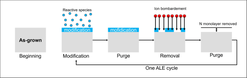
The ALE framework alternates sequentially between surface modification and physical removal, utilizing a low-power strike step for igniting the Ar plasma without reflected power spikes. The cyclic process begins with a gentle O₂ modification step that oxidizes the carbon surface, followed by an in-situ chamber gas purge to stabilize chamber pressure and clear unreacted radicals. Directional Ar⁺ ion bombardment then selectively desorbs the modified surface layer, self-terminating once the unmodified pristine diamond surface is exposed, prior to a final purge step.
Two synergistic mechanisms drive this continuous process: the oxidative etching of an amorphous carbon (a-C) overlayer that ends in oxygen termination, and the physical desorption of COx followed by the creation of a finite a-C overlayer with an estimated depth of 0.4 ± 0.1 nm.
Recipe Optimization & Parameter Sweeps
Establishing a true ALE operating window required systematically decoupling chemical modification from physical sputtering across ICP-RIE tools. From there, sweeping RF power directly revealed an ALE regime with a controlled Etch Per Cycle (EPC) of 0.8 nm/cycle.
Process monitoring and etch rate determination were conducted on non-overgrown single-crystal diamonds using Filmometrics ES-4 ellipsometry and reflectometry to measure precise pre-etch and post-etch thickness across hundreds of continuous cycles.
Surface Smoothing & Chemical Metrology
Characterization performed using Scanning Electron Microscopy (SEM), Atomic Force Microscopy (AFM), X-ray Photoelectron Spectroscopy (XPS), and Angle-Resolved XPS (ARXPS) confirmed exceptional surface smoothing. Performing an ICP-RIE pre-etch followed by our ALE recipe on DDK-polished and SmartCut diamonds reliably produced atomic smoothness, reducing surface RMS roughness (Rq) down to less than 50 pm over a 500 nm x 500 nm scan area.